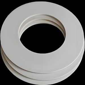
Next-Generation Ceramics: Unlocking Superior Properties for Industry
PRODUCT PARAMETERS
Description
Overview of 170 W/mK Machinable Customized Aluminum Nitride Wafer
Aluminum Nitride (AlN) is a premier technical ceramic engineered for exceptional thermal management and electrical insulation. Its standout feature is its very high thermal conductivity, rivaling that of metals like beryllium oxide but without the toxicity, making it the material of choice for high-power and high-frequency electronic applications.
Features of 170 W/mK Machinable Customized Aluminum Nitride Wafer
- Very High Thermal Conductivity: Excellent heat dissipation (140-180 W/mK), critical for managing thermal loads in electronics.
- Electrical Insulator: Superior dielectric properties and high electrical resistivity.
- Coefficient of Thermal Expansion (CTE) Matching Silicon: Closely matches the CTE of silicon chips, minimizing thermal stress in semiconductor packaging.
- Non-Toxic: A safe alternative to toxic beryllium oxide (BeO) ceramics.
- Good Mechanical Strength: Possesses adequate strength and hardness for structural support in electronic packages.
Specification of 170 W/mK Machinable Customized Aluminum Nitride Wafer
170 W/mK Machinable Personalized Light Weight Aluminum Nitride Wafer
High Thermal Conductivity for Requiring Applications
This aluminum nitride (AlN) wafer supplies a thermal conductivity of 170 W/mK , making it excellent for high-power electronic devices and thermal monitoring systems. It relocates warm away quickly and efficiently, which helps gadgets run cooler and last much longer.
Precision Machining for Exact Fit
We provide completely tailored measurements and shapes to match your precise layout demands. The product is machinable with standard devices, so you get tight resistances without additional cost or delay. Whether you require round, square, or facility geometries, we can create it accurately.
Exceptional Electric Insulation
Alongside its strong warm transfer capacity, this AlN wafer gives high electric resistivity . It works as an efficient insulator even at raised temperatures. This twin efficiency makes it ideal for use in power components, LED substratums, RF elements, and semiconductor packaging.
Stable Performance Throughout Temperatures
The wafer preserves its mechanical stamina and thermal buildings from space temperature as much as over 1000 ° C in inert atmospheres. Its reduced coefficient of thermal expansion carefully matches silicon and various other usual semiconductors, reducing tension during thermal cycling.
Tidy and Reliable Material
Our aluminum nitride wafers are made with high-purity basic materials and strict procedure control. They have reduced oxygen web content , which guarantees constant thermal performance and minimizes issues. Each batch meets sector criteria for pureness, thickness, and surface finish.
All set for Assimilation
These wafers integrate efficiently right into existing production lines. Surface alternatives include as-fired, lapped, or refined finishes, relying on your bonding or placing needs. We sustain quick prototyping and volume production with constant top quality.
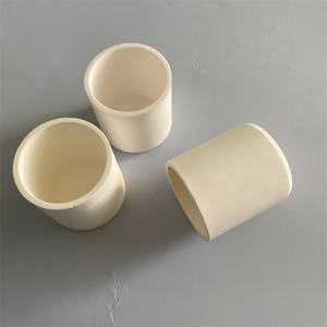
Applications of 170 W/mK Machinable Customized Aluminum Nitride Wafer
Applications of 170 W/mK Machinable Personalized Light Weight Aluminum Nitride Wafer
High-Power Electronics Need Better Warmth Control
Light weight aluminum nitride (AlN) wafers with a thermal conductivity of 170 W/mK offer excellent warm dissipation. This makes them excellent for high-power electronic gadgets that produce a lot of warm. Unlike typical materials, AlN moves warm away promptly and maintains components cool down during procedure.
Made use of in LED and Laser Solutions
In high-brightness LED illumination and laser diodes, temperature level control is critical. These systems rely on customized AlN wafers to keep steady efficiency. The product’s electric insulation and thermal efficiency avoid getting too hot and prolong device life.
Suitable for RF and Microwave Gadgets
Superhigh frequency (RF) and microwave parts demand both thermal management and signal honesty. The 170 W/mK AlN wafer offers low dielectric loss and strong thermal conduction. Engineers use it as a substrate in power amplifiers, radar components, and 5G infrastructure.
Sustains Advanced Semiconductor Product Packaging
As chips get smaller and extra powerful, handling warmth ends up being harder. Machinable AlN wafers can be formed to fit complex packaging designs. Their compatibility with typical fabrication procedures permits seamless combination right into next-generation semiconductor modules.
Reputable in Rough Atmospheres
AlN wafers work well under severe problems. They stand up to thermal shock, remain secure at high temperatures, and do not break down quickly. This dependability makes them useful in aerospace, protection, and commercial applications where failure is not an alternative.
Personalized Shapes Meet Certain Needs
Every task has one-of-a-kind demands. The customized nature of these wafers implies they can be reduced, pierced, or brightened to exact dimensions. This flexibility sustains fast prototyping and customized production without giving up efficiency.

Company Profile
Synthetic-chemical. focus on the research and development, production and sales of ceramic products, serving the electronics, ceramics, chemical and other industries. Since its establishment in 2015, the company has been committed to providing customers with the best products and services, and has become a leader in the industry through continuous technological innovation and strict quality management.
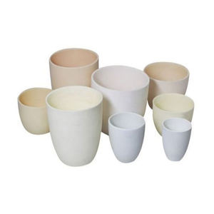
Our products includes but not limited to Aluminum Nitride, Aluminum Oxide, Boron Carbide, Boron Nitride, Ceramic Crucible, ect. If you are interested in any type of these, please feel free to contact us.

Payment Methods
T/T, Western Union, Paypal, Credit Card etc.
Shipment Methods
By air, by sea, by express, as customers request.
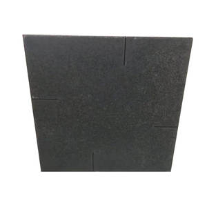
5 FAQs of 170 W/mK Machinable Customized Aluminum Nitride Wafer
Frequently Asked Questions: 170 W/mK Machinable Customized Aluminum Nitride Wafer
What is aluminum nitride (AlN) used for?
Aluminum nitride wafers are used in high-power electronics, LED lighting, and RF devices. They handle heat well and insulate electricity. This makes them ideal where heat must move away fast but electrical isolation is still needed.
Why choose a thermal conductivity of 170 W/mK?
A value of 170 W/mK means the material moves heat very efficiently. It works better than many standard ceramics. This level of performance helps keep electronic parts cool and stable during heavy use.
Can you machine aluminum nitride to custom shapes?
Yes. These wafers can be cut, drilled, or shaped to your exact design. We use special tools to avoid cracking. The result is a precise part that fits your system without extra hassle.
Is aluminum nitride fragile?
It is a ceramic, so it is harder than metal but more brittle. Handle it with care during assembly. Once installed properly, it performs reliably under normal operating conditions.
How does AlN compare to alumina or beryllium oxide?
AlN offers much higher thermal conductivity than alumina—about 10 times better. Unlike beryllium oxide, it is non-toxic and safe to handle. This gives AlN a strong edge in both performance and safety for modern electronics.
REQUEST A QUOTE
RELATED PRODUCTS
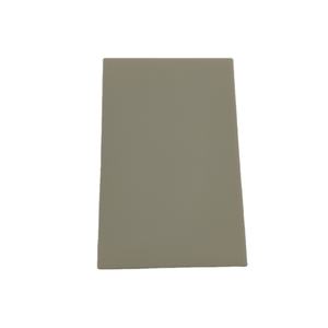
Advanced Durable Aluminum Nitride Ceramics for Electronic Devices
High Purity 99.9% Aluminum Nitride Powder for Ceramics Factory 10um
Hot High Purity Aluminum Nitride for Integrated Circuit Substrates
Factory Wear Resistance MOSFET IGBT Aluminum Nitride Thermal Pad Substrate with Hole
99.9% Purity Alumina Ceramic Ball Grinding Media and Related Materials