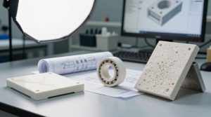
Next-Generation Ceramics: Unlocking Superior Properties for Industry
PRODUCT PARAMETERS
Description
Overview of Boron Nitride Ceramic for Semiconductor Material
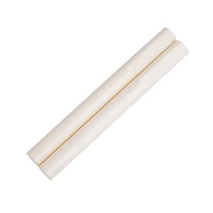
Boron Nitride (BN) exists in multiple polymorphs, with Hexagonal Boron Nitride (h-BN) being the most common ceramic form. Often called “white graphite” due to its similar layered, lubricious structure, it is distinguished by its exceptional thermal stability, electrical insulation, and chemical inertness, even at extreme temperatures.
Features of Boron Nitride Ceramic for Semiconductor Material
- High Thermal Conductivity & Excellent Electrical Insulation: Unique combination that allows it to conduct heat like a metal but insulate like a ceramic.
- Outstanding Thermal Shock Resistance: Can be heated and cooled rapidly without cracking.
- Natural Lubricity: Exhibits low friction and anti-stick properties, even at high temperatures.
- Chemically Inert: Resists wetting by and reaction with most molten metals, slags, and glasses.
- Machinable: Unlike most advanced ceramics, h-BN in its solid form can be machined to precision tolerances using conventional carbide tooling.
Specifications of Boron Nitride Ceramic for Semiconductor Material
Specs of Boron Nitride Ceramic for Semiconductor Applications
Material Composition and Purity
Boron nitride (BN) ceramic made use of in semiconductor manufacturing is made from high-purity hexagonal boron nitride (h-BN). The product commonly contains over 99% BN , with very little contaminations such as oxygen, carbon, or metallic elements. This level of purity helps stop contamination during delicate fabrication procedures.
Thermal Qualities
This ceramic programs excellent thermal security. It can run continuously at temperature levels as much as 1000 ° C in air and also higher in inert atmospheres. Its thermal conductivity ranges from 30 to 60 W/m · K , depending on thickness and orientation. In spite of this, it remains an electrical insulator, which is necessary for semiconductor tools and components.
Electrical Qualities
Boron nitride ceramic is a solid electrical insulator. Its volume resistivity surpasses 10 ¹⁴ Ω · cm at room temperature. Dielectric stamina is usually above 30 kV/mm . These homes make it excellent for usage in wafer handling elements, protecting spacers, and plasma chamber parts where roaming currents should be avoided.
Mechanical and Chemical Actions
The material is soft compared to other porcelains, with a Mohs firmness of regarding 2 , enabling very easy machining right into complex forms. It withstands attack from many liquified metals and acids, though it may weaken in solid oxidizing settings at heats. Its low coefficient of thermal development ( 2– 3 × 10 ⁻⁶/ ° C ) makes certain dimensional stability throughout thermal biking.
Trick Features for Semiconductor Usage
– Non-wetting surface area prevents adhesion of liquified materials
– Reduced fragment generation minimizes threat of wafer contamination
– High pureness and chemical inertness sustain cleanroom compatibility
– Machinable prior to final sintering , allowing tight resistances
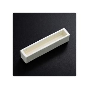
These attributes make boron nitride ceramic a trusted choice for crucibles, susceptors, insulators, and various other critical components in semiconductor assembly line.
Applications of Boron Nitride Ceramic for Semiconductor Material
Applications of Boron Nitride Ceramic in Semiconductor Production
Why Boron Nitride Sticks Out
Boron nitride ceramic is extensively made use of in the semiconductor industry. It has solid heat resistance and stays secure also at really heats. This material does not react quickly with other chemicals. That makes it risk-free to use around delicate electronic parts.
Thermal Management
Warm control is crucial throughout chip manufacturing. Boron nitride conducts warm well but does not conduct power. Designers utilize it in elements like wafer chucks and heating unit plates. These components need to remain amazing and steady while taking care of wafers. Boron nitride helps avoid overheating without triggering brief circuits.
Clean Handling Atmospheres
Semiconductor manufacture needs ultra-clean problems. Even tiny bits can spoil a chip. Boron nitride releases practically no impurities when heated. It is typically shaped right into insulators, spacers, or crucibles inside vacuum chambers. Its smooth surface area also stands up to bit buildup.
Machinability and Resilience
This ceramic is simple to shape right into complicated parts. It can be machined specifically without splitting. At the exact same time, it holds up well under duplicated thermal cycling. Devices made from boron nitride last much longer and lower downtime in assembly line.
Compatibility with Advanced Processes
As chips get smaller and more powerful, producing needs expand more stringent. Boron nitride functions well in plasma etching and chemical vapor deposition systems. It stands up to hostile gases and high-energy environments much better than lots of various other porcelains. This reliability sustains next-generation semiconductor modern technologies.
Producers trust boron nitride ceramic since it addresses numerous challenges simultaneously. It keeps processes tidy, manages warm safely, and fits into limited spaces without failing. These top qualities make it a vital product in modern chip-making tools.

Company Profile
Synthetic-chemical focus on the research and development, production and sales of ceramic products, serving the electronics, ceramics, chemical and other industries. Since its establishment in 2015, the company has been committed to providing customers with the best products and services, and has become a leader in the industry through continuous technological innovation and strict quality management.
Our products includes but not limited to Aluminum Nitride, Aluminum Oxide, Boron Carbide, Boron Nitride, Ceramic Crucible, ect. If you are interested in any type of these, please feel free to contact us.

Payment Methods
T/T, Western Union, Paypal, Credit Card etc.
Shipment Methods
By air, by sea, by express, as customers request.
5 FAQs of Boron Nitride Ceramic for Semiconductor Material
Frequently Asked Questions About Boron Nitride Ceramic for Semiconductor Use
What is boron nitride ceramic?
Boron nitride ceramic is a high-performance material made from boron and nitrogen. It comes in different forms, but the hexagonal type is most common in semiconductors. This ceramic resists heat well, does not conduct electricity, and stays stable even at very high temperatures.
Why is it used in semiconductor manufacturing?
Semiconductor processes need materials that handle extreme heat without reacting with other chemicals. Boron nitride ceramic fits this need. It insulates electrical parts, supports wafers during processing, and helps control temperature evenly across tools.
How does it compare to other ceramics?
Compared to alumina or quartz, boron nitride has better thermal shock resistance and lower thermal expansion. It also releases fewer particles during use. These traits help keep semiconductor production clean and reduce defects on chips.
Is it safe for cleanroom environments?
Yes. Boron nitride ceramic meets cleanroom standards. It does not shed dust easily and stays chemically inert when exposed to aggressive gases like chlorine or fluorine. This makes it reliable inside sensitive fabrication areas.
Can it be machined into complex shapes?
Yes. Even though it is hard, boron nitride can be shaped into custom parts like crucibles, insulators, or wafer chucks. Manufacturers often machine it before final sintering to get tight tolerances needed in semiconductor equipment.
REQUEST A QUOTE
RELATED PRODUCTS
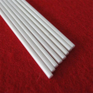
Boron Nitride Ceramic Assembled Parts for Sintering Phosphor
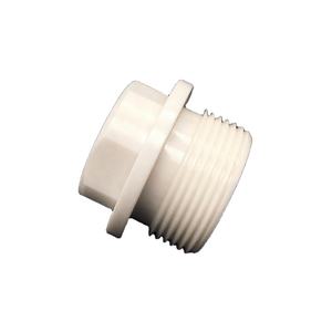
Boron Nitride Ceramic Ring High Thermal Shock Resistance

Boron Nitride Ceramic Tube High Temperature Corrosion Resistant
High Purity Boron Nitride for Electronic Ceramics
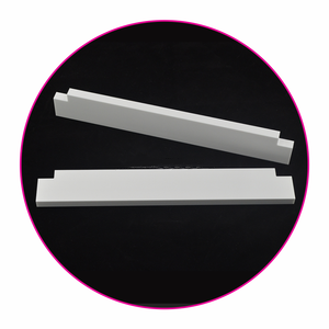
High Performance Boron Nitride Ceramic Pipe Industrial Use