Next-Generation Ceramics: Unlocking Superior Properties for Industry
PRODUCT PARAMETERS
Description
Overview of Metallized AIN Substrate with AMB Technology and OSP Treatment
Aluminum Nitride (AlN) is a premier technical ceramic engineered for exceptional thermal management and electrical insulation. Its standout feature is its very high thermal conductivity, rivaling that of metals like beryllium oxide but without the toxicity, making it the material of choice for high-power and high-frequency electronic applications.
Features of Metallized AIN Substrate with AMB Technology and OSP Treatment
- Very High Thermal Conductivity: Excellent heat dissipation (140-180 W/mK), critical for managing thermal loads in electronics.
- Electrical Insulator: Superior dielectric properties and high electrical resistivity.
- Coefficient of Thermal Expansion (CTE) Matching Silicon: Closely matches the CTE of silicon chips, minimizing thermal stress in semiconductor packaging.
- Non-Toxic: A safe alternative to toxic beryllium oxide (BeO) ceramics.
- Good Mechanical Strength: Possesses adequate strength and hardness for structural support in electronic packages.
Specification of Metallized AIN Substrate with AMB Technology and OSP Treatment
This metallized light weight aluminum nitride substratum utilizes AMB innovation. It begins with a high-purity AlN ceramic base. This base has excellent thermal conductivity. It relocates heat away fast. Active Metal Brazing bonds thick copper layers directly onto the AlN. AMB produces a solid bond. This bond manages high temperatures well. The copper layers are thick. They carry high currents quickly. This substrate is very flat. Flatness is essential forever setting up. The surface gets an OSP therapy. OSP is a natural solderability chemical. This covering protects the copper. It stops oxidation prior to assembly. The OSP layer liquifies during soldering. This leaves a clean copper surface area. Tidy copper makes strong solder joints. Strong joints imply trustworthy links. This substrate operates in challenging areas. It manages high power and high heat. You find it in power components. These consist of IGBTs and SiC tools. It is also great for EV power systems. High-reliability industrial equipment uses it too. AMB technology offers it strength. The AlN base relocates warmth effectively. OSP keeps the surface prepared for soldering. This combination offers leading performance. It fulfills the needs of contemporary electronic devices. Power thickness maintains increasing. Heat management is critical. This substrate helps fix that problem. It sustains the most recent semiconductor technology. It offers a stable mounting surface area. Designers trust it for crucial applications. It supplies consistent results. The products and processes are verified.
Applications of Metallized AIN Substrate with AMB Technology and OSP Treatment
Light weight aluminum nitride (AlN) substratums are wonderful for electronic devices requiring to handle great deals of warm. Metallization places a copper layer on the AIN surface. This copper layer allows you attach digital components conveniently. AMB modern technology bonds the copper to the AIN very strongly. This strong bond is important for tough problems. It stops the layers from separating under stress. OSP treatment layers the copper surface area. This covering secures the copper from rusting prior to you utilize it. OSP likewise makes soldering parts onto the copper a lot easier. It assists produce dependable electrical links.
These substratums are perfect for high-power electronics. Think of devices like IGBT components utilized in trains or manufacturing facilities. They likewise work well in power converters for renewable energy systems. These applications produce a lot of warm. The AIN material moves heat away from sensitive parts quickly. This maintains whatever running cooler and extra accurately. The metallized surface area supplies excellent electric pathways. AMB makes certain the whole structure remains undamaged despite having temperature changes. OSP makes assembly much faster and extra reliable. You get regular solder joints whenever.
RF and microwave tools additionally make use of these substrates. Components like power amplifiers need secure systems. The low electrical loss of AIN is a big benefit below. Signal stability stays high. The thermal administration quits hotspots from developing. This is crucial for efficiency and life-span. LED lighting systems benefit as well. High-brightness LEDs need reliable air conditioning. Metallized AIN substrates manage the warm efficiently. This assists LEDs last longer and remain brighter.
Automotive electronic devices rely on resilient materials. Electric vehicle power systems face rough environments. Metallized AIN with AMB can take care of the vibration and heat. OSP makes sure good solder connections endure lasting usage. These substrates provide a solid option. They combine wonderful warmth spreading with strong electrical performance. The manufacturing process is durable due to AMB and OSP. You end up with a trusted, high-performance product. It satisfies the demands of modern power electronic devices.

Company Profile
Synthetic-chemical. focus on the research and development, production and sales of ceramic products, serving the electronics, ceramics, chemical and other industries. Since its establishment in 2015, the company has been committed to providing customers with the best products and services, and has become a leader in the industry through continuous technological innovation and strict quality management.
Our products includes but not limited to Aluminum Nitride, Aluminum Oxide, Boron Carbide, Boron Nitride, Ceramic Crucible, ect. If you are interested in any type of these, please feel free to contact us.

Payment Methods
T/T, Western Union, Paypal, Credit Card etc.
Shipment Methods
By air, by sea, by express, as customers request.
5 FAQs of Metallized AIN Substrate with AMB Technology and OSP Treatment
What is Metallized AIN Substrate with AMB Technology and OSP Treatment?
This is a special kind of circuit board base. It uses aluminum nitride ceramic. AMB technology bonds copper directly onto this ceramic. OSP is a thin coating applied to the copper surface. This coating prevents oxidation before soldering.
Why use AMB Technology?
AMB creates a very strong bond. The copper sticks extremely well to the aluminum nitride. This bond is vital for moving heat away quickly. Good heat removal protects sensitive electronics. It stops parts from getting too hot and failing.
What does OSP Treatment do?
OSP stands for Organic Solderability Preservative. It protects the exposed copper surfaces. Without OSP, copper can oxidize quickly in air. Oxidation makes soldering difficult or impossible. OSP keeps the copper fresh and ready for soldering until assembly.
What are the main advantages?
This substrate offers excellent thermal performance. Aluminum nitride moves heat better than many other materials. The strong AMB bond ensures heat flows out efficiently. OSP guarantees reliable solder connections during manufacturing. It combines high power handling with dependable assembly.
Where is this substrate typically used?
It is ideal for high-power electronics needing good cooling. You find it in power modules for electric cars. It’s used in industrial motor drives. High-brightness LED lighting systems use it. Advanced radio frequency power amplifiers benefit from it. Any application pushing lots of power and needing efficient cooling is a good fit.
REQUEST A QUOTE
RELATED PRODUCTS
Non Magnetic Insulated Aluminum Nitride Ceramic Crucible
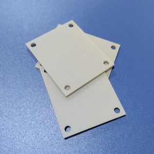
Customize Different Shape Aluminum Nitride Ceramic Parts and Components
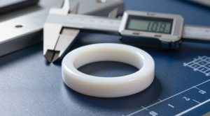
High Purity 99.5% Aluminum Nitride Sputtering Target for Thin Film Deposition
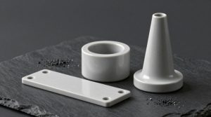
Customized Precision Aluminum Nitride Insulating Ceramic Parts Mechanical Components
Standard Aluminum Nitride Ceramic Tube