Next-Generation Ceramics: Unlocking Superior Properties for Industry

PRODUCT PARAMETERS
Description
Overview of Laser Drilled Alumina (Al2O3) Ceramic PCB Substrate
Alumina Ceramic, or Aluminum Oxide (Al₂O₃), is the most widely used and versatile advanced ceramic material. Known for its excellent balance of mechanical, thermal, and electrical properties, it is a cost-effective solution for a vast array of demanding industrial applications. Alumina components are produced in purity levels ranging from 85% to 99.9%, with properties enhancing as purity increases.
Features of Laser Drilled Alumina (Al2O3) Ceramic PCB Substrate
- High Hardness & Wear Resistance: Offers exceptional resistance to abrasion and mechanical wear.
- Excellent Electrical Insulation: Maintains high electrical resistivity even at elevated temperatures.
- Good Thermal Conductivity: (For a ceramic) effectively dissipates heat, especially in higher purity grades.
- High Compressive Strength: Capable of withstanding significant mechanical loads.
- Chemical Inertness: Highly resistant to corrosion from acids, alkalis, and molten metals.
- Cost-Effectiveness: Provides superior performance at a lower cost compared to many other technical ceramics.
Specifications of Laser Drilled Alumina (Al2O3) Ceramic PCB Substrate
Specs of Laser Drilled Alumina (Al Two O FOUR) Ceramic PCB Substrate
Product Composition
Laser drilled alumina ceramic PCB substratums are made from high-purity light weight aluminum oxide (Al two O SIX). The conventional purity level is 96%, yet choices with 99.5% purity are additionally available for applications that need better electric insulation or thermal efficiency.
Density and Measurements
The substratum density typically ranges from 0.25 mm to 1.0 mm. Customized sizes can be generated, however usual panel dimensions consist of 100 mm × 100 mm and 150 mm × 150 mm. Thickness tolerance is held within ± 0.05 mm to make certain regular performance in setting up and operation.
Laser Drilling Includes
Micro-vias are produced utilizing precision laser boring. Opening sizes start as small as 50 microns and can increase to 300 microns, depending upon layout requirements. The procedure enables limited control over hole positioning, with positional precision far better than ± 10 microns. Through-holes, blind vias, and buried vias are all possible.
Thermal and Electric Qualities
Alumina substrates provide solid thermal conductivity– normally between 24– 28 W/m · K for 96% pureness product. They additionally offer excellent electric insulation, with a dielectric strength of over 15 kV/mm. The coefficient of thermal expansion (CTE) has to do with 6.8 ppm/ ° C, which closely matches several semiconductor products. This helps in reducing anxiety throughout thermal cycling.
Surface Area and Complete Choices
The surface finish is smooth, with a roughness (Ra) under 0.5 µm. Metallization layers such as thick-film silver, gold, or copper can be added. These layers support cable bonding, soldering, or direct component placing. Side damaging is decreased via mindful handling and dicing methods.
Mechanical Stamina
These substratums are difficult and rigid. Flexural strength normally surpasses 300 MPa, making them ideal for demanding settings. They resist wetness, chemicals, and heats approximately 1600 ° C in non-load conditions.
Applications of Laser Drilled Alumina (Al2O3) Ceramic PCB Substrate
Applications of Laser Drilled Alumina (Al ₂ O THREE) Ceramic PCB Substratums
High-Power Electronic devices
Laser pierced alumina ceramic PCB substrates manage high power far better than conventional materials. They spread out warm quickly and remain stable under heavy electric tons. This makes them excellent for power components, inverters, and motor drives made use of in electric automobiles and commercial devices.
LED Lighting Systems
In LED illumination, warmth control is vital. Alumina substratums with laser-drilled vias relocate heat away from the LED chips promptly. This maintains light outcome strong and extends product life. Streetlights, vehicle fronts lights, and high-brightness indoor fixtures all gain from this technology.
Aerospace and Protection
Aerospace systems demand dependability in tough conditions. Laser pierced alumina PCBs stand up to vibration, severe temperatures, and radiation. They are made use of in radar devices, interaction equipment, and onboard electronic devices where failure is not an alternative.
Medical Gadgets
Medical devices need clean, compact, and trustworthy circuitry. Alumina’s biocompatibility and electric insulation suit medical tools, imaging systems, and implantable devices. Precision laser exploration enables limited component placement without compromising efficiency.
RF and Microwave Circuits
For radio frequency applications, signal clarity issues. Alumina offers reduced signal loss and constant dielectric buildings. Laser boring creates accurate using paths that preserve signal stability in antennas, filters, and 5G facilities.
Sensing Units and Harsh Setting Electronic Devices
Sensing units in oil and gas, automotive, or producing setups face heat, chemicals, and stress. Alumina ceramic substratums endure these difficulties. Their laser-formed micro-vias assistance dense circuit layouts while keeping links trusted.

Company Profile
Synthetic-chemical focus on the research and development, production and sales of ceramic products, serving the electronics, ceramics, chemical and other industries. Since its establishment in 2015, the company has been committed to providing customers with the best products and services, and has become a leader in the industry through continuous technological innovation and strict quality management.
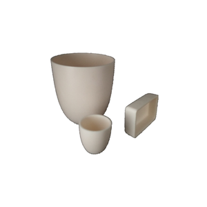
Our products includes but not limited to Aluminum Nitride, Aluminum Oxide, Boron Carbide, Boron Nitride, Ceramic Crucible, ect. If you are interested in any type of these, please feel free to contact us.

Payment Methods
T/T, Western Union, Paypal, Credit Card etc.
Shipment Methods
By air, by sea, by express, as customers request.
5 FAQs of Laser Drilled Alumina (Al2O3) Ceramic PCB Substrate
Frequently Asked Questions About Laser Drilled Alumina (Al₂O₃) Ceramic PCB Substrates
What is a laser drilled alumina ceramic PCB substrate?
It is a circuit board base made from high-purity aluminum oxide (Al₂O₃). Tiny holes are created using a precise laser instead of mechanical drilling. This method gives clean, accurate vias without cracking the brittle ceramic material.
Why use laser drilling instead of mechanical drilling?
Alumina ceramic is very hard and fragile. Mechanical drills often cause micro-cracks or chipping. Laser drilling avoids physical contact, so it produces smoother hole walls and better alignment. It also allows smaller hole sizes that mechanical tools cannot achieve.
What are the main benefits of alumina ceramic substrates?
They handle high heat well and do not expand much when heated. They also insulate electricity effectively and stay stable in harsh environments. These traits make them ideal for power electronics, LED lighting, and automotive sensors.
Can these substrates support fine circuit patterns?
Yes. The smooth surface of laser-drilled alumina allows thin copper traces to be printed clearly. This supports dense layouts needed in modern compact devices. The precision of laser vias also helps connect layers accurately without short circuits.
Are laser drilled alumina PCBs more expensive?
They cost more than standard FR-4 boards because of the material and laser process. But their performance in high-power or high-temperature applications often justifies the price. They reduce system failures and extend product life, which lowers long-term costs.
REQUEST A QUOTE
RELATED PRODUCTS
99.99% Purity Alumina Ceramic Sputtering Target – Custom Sizes
Alumina Ceramic Raschig Ring for Chemical Filling & Catalyst Support
Zirconia-Gravel Infused Alumina Ceramic Basket Gemstone – 38.1x25x23mm
High Purity 99.5% Al2O3 Ceramic Insulation Bushing
Low Sodium Microcrystalline Alumina Powder for Refractory Materials