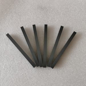
Next-Generation Ceramics: Unlocking Superior Properties for Industry
PRODUCT PARAMETERS
Description
Overview of Boron Nitride Aluminum Nitride Ceramics for Semiconductor
Boron Nitride (BN) exists in multiple polymorphs, with Hexagonal Boron Nitride (h-BN) being the most common ceramic form. Often called “white graphite” due to its similar layered, lubricious structure, it is distinguished by its exceptional thermal stability, electrical insulation, and chemical inertness, even at extreme temperatures.
Features of Boron Nitride Aluminum Nitride Ceramics for Semiconductor
- High Thermal Conductivity & Excellent Electrical Insulation: Unique combination that allows it to conduct heat like a metal but insulate like a ceramic.
- Outstanding Thermal Shock Resistance: Can be heated and cooled rapidly without cracking.
- Natural Lubricity: Exhibits low friction and anti-stick properties, even at high temperatures.
- Chemically Inert: Resists wetting by and reaction with most molten metals, slags, and glasses.
- Machinable: Unlike most advanced ceramics, h-BN in its solid form can be machined to precision tolerances using conventional carbide tooling.
Specifications of Boron Nitride Aluminum Nitride Ceramics for Semiconductor
Specs of Boron Nitride and Light Weight Aluminum Nitride Ceramics for Semiconductor Applications
Material Structure and Pureness
These porcelains are made from high-purity boron nitride (BN) or light weight aluminum nitride (AlN). BN grades usually contain over 99% hexagonal boron nitride. AlN products use purity levels over 99.5%, with regulated oxygen web content below 1%. Both products are devoid of metal contaminations that can harm semiconductor performance.
Thermal Characteristics
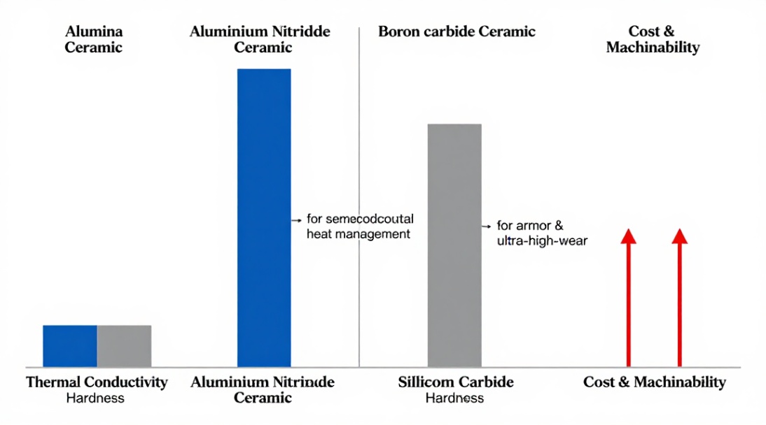
Light weight aluminum nitride shows exceptional thermal conductivity– ranging from 140 to 180 W/m · K– making it ideal for warm dissipation in power tools. Boron nitride has reduced thermal conductivity (30– 60 W/m · K) however offers strong electrical insulation and steady performance across large temperature level arrays. Both products take care of operating temperature levels up to 800 ° C in air and also greater in inert ambiences.
Electric Features
Both porcelains serve as electric insulators. BN has a volume resistivity above 10 ¹⁴ Ω · cm. AlN maintains resistivity over 10 ¹³ Ω · centimeters, even at raised temperatures. Their dielectric constants stay low– around 4 for BN and 8– 9 for AlN– sustaining high-frequency signal stability in semiconductor packaging.
Mechanical and Chemical Security
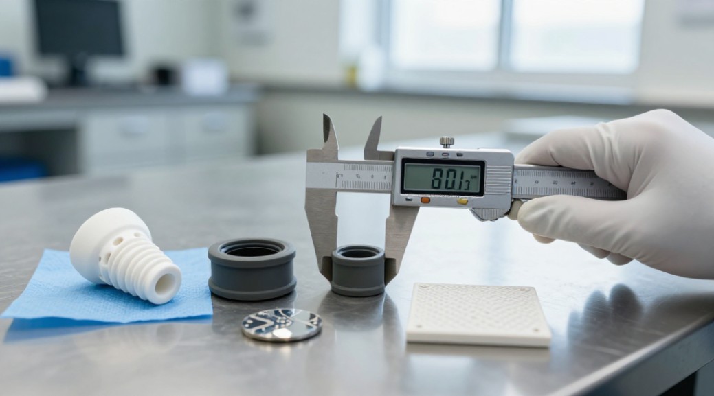
These porcelains are hard, stiff, and immune to thermal shock. They do not react with many molten steels or semiconductor procedure gases. BN provides lubricity and simple machinability, while AlN provides greater mechanical stamina. Both products keep dimensional security throughout repeated thermal biking.
Applications in Semiconductor Manufacturing
They are utilized in wafer chucks, insulating spacers, heating unit plates, and chamber linings. BN’s non-wetting surface avoids product build-up during deposition. AlN’s high thermal conductivity aids handle warm in RF and power components. Each product is selected based on specific thermal, electrical, and mechanical requirements in cleanroom settings.
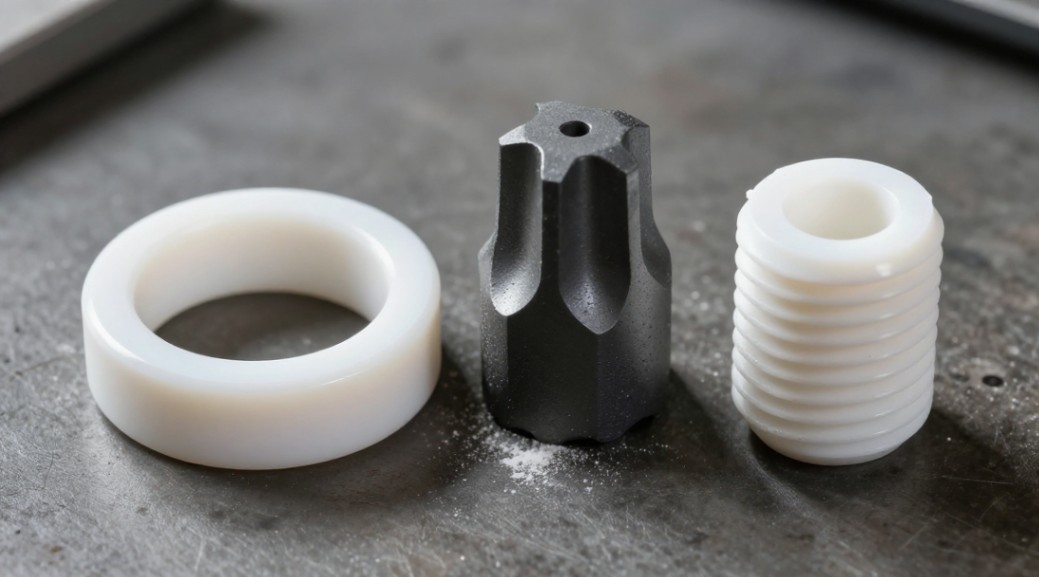
Applications of Boron Nitride Aluminum Nitride Ceramics for Semiconductor
Applications of Boron Nitride and Aluminum Nitride Ceramics in Semiconductor Manufacturing
Thermal Management Solutions
Semiconductor gadgets create a great deal of heat throughout procedure. If this warmth is not eliminated rapidly, efficiency declines and parts can stop working. Boron nitride (BN) and aluminum nitride (AlN) ceramics use superb thermal conductivity while remaining electrically protecting. This makes them excellent for warm spreaders, substrates, and shielding layers in power electronic devices. AlN, particularly, conducts warmth much better than the majority of various other ceramic insulators, aiding chips remain great under hefty tons.
Accuracy Components for Wafer Processing
Throughout chip construction, wafers go through extreme temperatures and corrosive chemicals. Basic steels or plastics can not endure these conditions. BN and AlN porcelains withstand high heat, do not react with hostile gases, and preserve their shape. They are used to make wafer chucks , susceptors , and shower heads inside plasma etch and deposition chambers. Their stability makes sure regular outcomes across countless manufacturing cycles.
Electric Insulation Without Signal Loss
Modern semiconductors operate at high frequencies. Any kind of product near the circuit have to not conflict with signals. BN and AlN have reduced dielectric loss, suggesting they do not take in or misshape electric signals. Designers use them in RF parts , packaging bases , and feedthrough insulators where signal quality issues. Their smooth surface areas likewise help reduce undesirable representations or sound.
Clean and Contamination-Free Performance
Even tiny particles or steel ions can wreck a semiconductor wafer. BN and AlN porcelains are ultra-pure and do not drop particles during usage. They also do not release dangerous vapors when heated. This tidiness is important in cleanroom atmospheres where return and dependability rely on overall control over materials. As chip styles obtain smaller, the need for such pure, stable porcelains just expands.

Company Profile
Synthetic-chemical focus on the research and development, production and sales of ceramic products, serving the electronics, ceramics, chemical and other industries. Since its establishment in 2015, the company has been committed to providing customers with the best products and services, and has become a leader in the industry through continuous technological innovation and strict quality management.
Our products includes but not limited to Aluminum Nitride, Aluminum Oxide, Boron Carbide, Boron Nitride, Ceramic Crucible, ect. If you are interested in any type of these, please feel free to contact us.

Payment Methods
T/T, Western Union, Paypal, Credit Card etc.
Shipment Methods
By air, by sea, by express, as customers request.
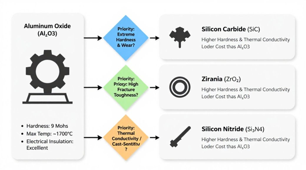
5 FAQs of Boron Nitride Aluminum Nitride Ceramics for Semiconductor
Frequently Asked Questions: Boron Nitride & Aluminum Nitride Ceramics for Semiconductor Applications
What makes boron nitride and aluminum nitride ceramics useful in semiconductors?
These ceramics handle heat very well. They also do not conduct electricity. This mix is perfect for semiconductor tools that must stay cool but stay electrically safe.
How do these materials help with thermal management?
Aluminum nitride moves heat quickly away from hot parts. Boron nitride spreads heat evenly without letting electricity pass through. Both keep sensitive components from overheating during production.
Are these ceramics compatible with harsh semiconductor processes?
Yes. They resist chemical attack from plasmas and cleaning gases used in chip making. They also hold up under high temperatures without breaking down or releasing contaminants.
Can they be shaped into complex parts?
Manufacturers can press and sinter both materials into precise shapes like wafer chucks, insulators, and focus rings. Their fine grain structure allows tight tolerances needed in modern fabs.
Why choose ceramic over metal or polymer parts?
Metals conduct electricity—this causes problems in plasma environments. Polymers melt or degrade at high heat. Boron nitride and aluminum nitride offer stability, purity, and performance where other materials fail.
REQUEST A QUOTE
RELATED PRODUCTS
Hot Pressing Boron Nitride Ceramic Insulating Board
Hot Pressed Boron Nitride Ceramic Part
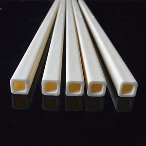
Custom Boron Nitride Ceramic for Electronic Devices High Temperature Resistant
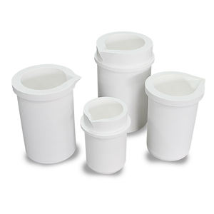
High Temperature Insulating Boron Nitride Ceramic Disc
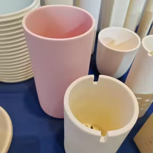
Boron Nitride Ceramic Tube Low Thermal Expansion